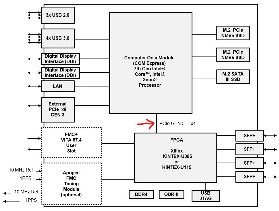
The Apogee Model 125 features a PCIe GEN 3 x4 lane bus to facilitate fast and easy data transfers between the FPGA and OS RAM. The FPGA uses custom Apogee FPGA IP Core and the Xilinx DMA/Bridge Subsystem for PCI Express. A new kernel level driver provides the interface to the Apogee FPGA IP Core and Xilinx IP Core. The new driver is called “apoxdmav”.
With apoxdmav users can utilize up to 32 Host-to-FPGA and 32 FPGA-to-Host “V-engines” (Virtual Engines) per Xilinx IP DMA/Bridge Engine. All 32 Host-to-FPGA and 32 FPGA-to-Host V-Engines can be running simultaneously and sharing the PCIe bus bandwidth. The typical maximum Total Byte Rate measured on the Model 125 PCIe bus is ~3.5 GB/sec in both directions simultaneously. Data sources could be things like ADC, DAC, DSP Programming streams, SDR Radio Software, and FMC Products.
As an example, with two V-Engines enabled- one V-Engine is receiving Analog to Digital converter data at a fixed 1 GB/sec rate. A second V-Engine started would have the remaining 2.5 GB/sec bus bandwidth available for use. The number of V-Engines enabled does not affect the % theoretical bus bandwidth, which remains at ~ 86% (as measured on the Model 125).
The FPGA IP can be configured for various numbers of V-Engines according the user’s needs. As an example, a user may only need four FPGA-to-Host and two Host-to-FPGA V-Engines for the project which will significantly reduce the required FPGA resources compared to a using all 32 in both directions. Simple C++ and Python APIs handle interactions between the kernel level driver and user programs.


